Services
Wafer Level Processes
Mask Design and Fabrication
Thin Film Deposition
Photolithography
Dry/Wet Etching
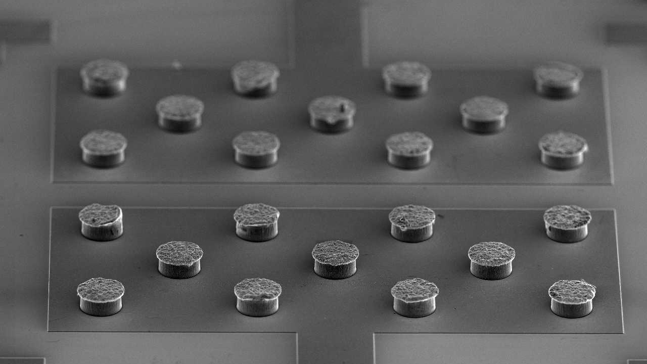
Plating (TSV, UBM, Solder, etc
Wafer Dicing
Chip/Package Level Processes
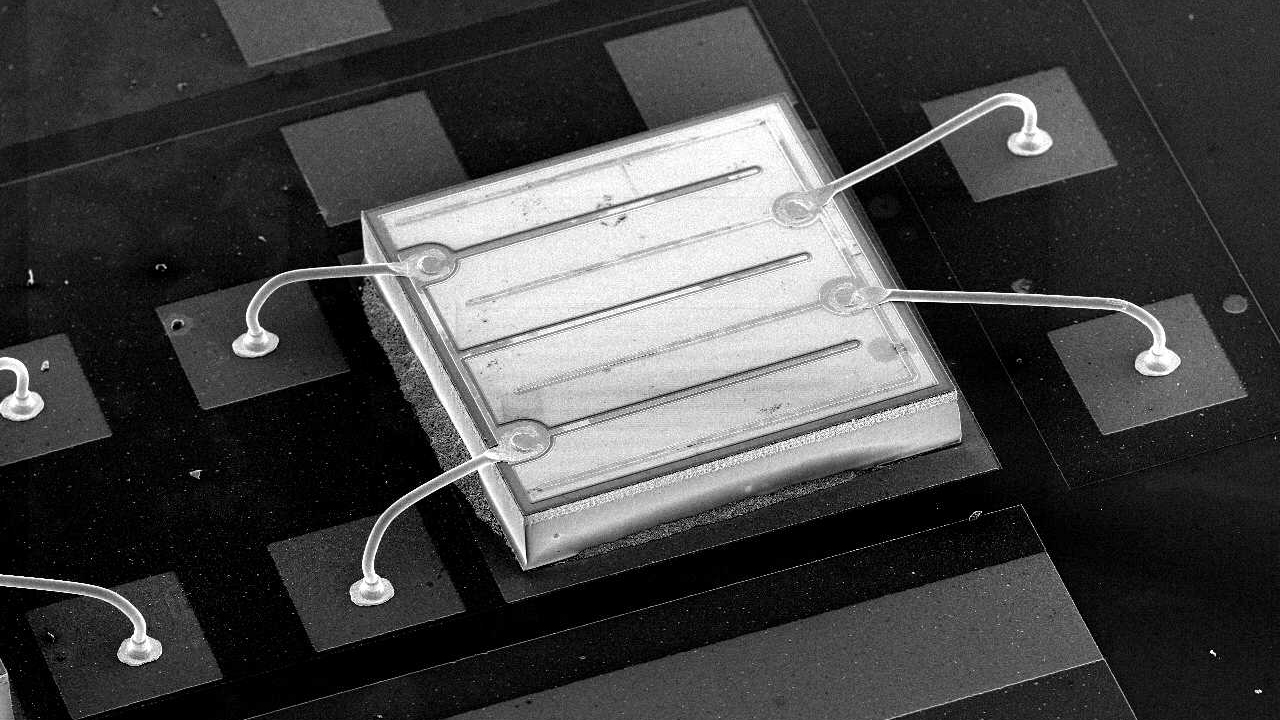
Die Bonding (Adhesive, Eutectic)
Wire Bonding (Au, Al, Cu)
Flip Chip Bonding (Thermo-compression, Thermo-sonic)
Underfill, Molding & Encapsulation
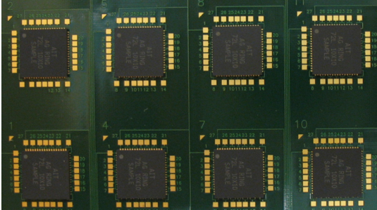
Board Level Processes
Substrate and PCB Layout Design
SMT Process
Rework
Material Characterizations & Inspection
DSC, DMA, TMA, TGA
Thermal Conductivity Measurement
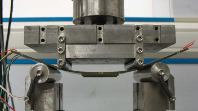
All UTM Related Testing
Roughness, Warpage Measurement
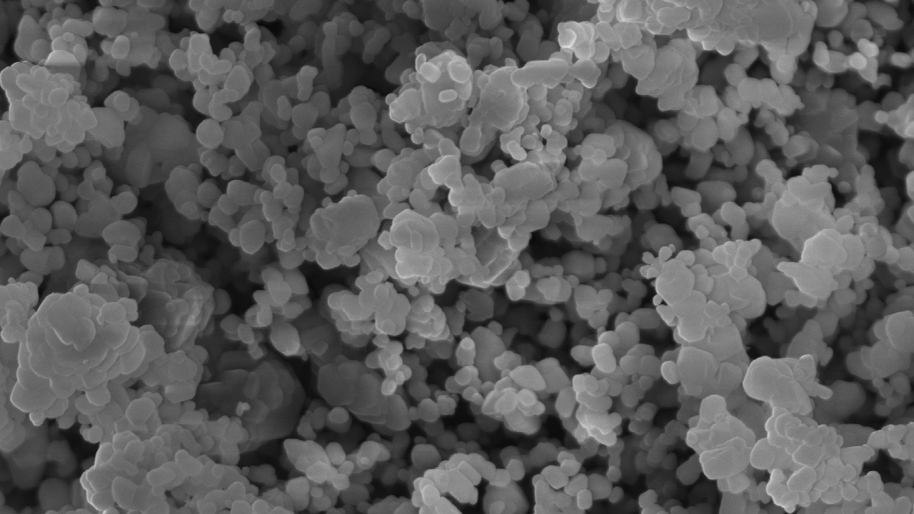
Particle Size Measurement
Reliability Assessment
Thermal Cycling
HAST
Moisture Sensitivity Level
Microtesting (Die Shear, Ball Pull/Shear, Wire Pull/Shear)
Bending (Monotonic, Cyclic)
Drop test
Failure Analysis
X-Ray
Scanning Acoustic Microscopy
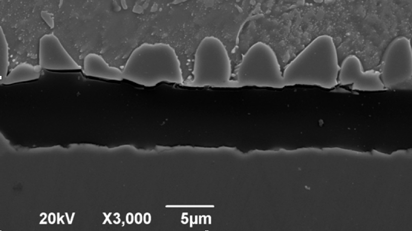
Cross-Section Inspection
SEM/EDX Inspection
Optical/Thermal Characterizations
Intergraing Sphere
Goniophotometer
Fluorescene Spectrometer
Thermal Transient Tester
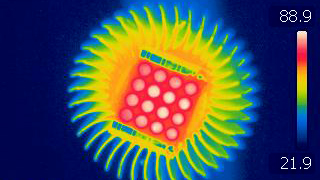
Infrared Thermal Imaging
Simulations
Mechanical
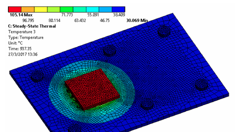
Thermal
Thermo-mechanical
Optical
R&D Collaboration
We welcome any R&D collaboration opportunties with local and international industries and/or research organizations. Government fundings may be applied jointly. Feel free to contact us for more details.