Projects
Additive Manufacturing of the Re-distribution Layer (RDL) for Rapid Prototyping of Chip-level Interconnection
The re-distribution layer (RDL) has been an enabling technology for wafer-level packaging. With RDL, the interconnection of ICs may be redefined for miniaturization and integration. Currently RDL relies on photolithography. This method can only be applied to whole wafers and not individual chips. However, during the development stage, microelectronics companies usually only get individual chips from foundries and not whole wafers. Consequently, they are unable to redistribute I/Os on the received chips using photolithography and must run redistribution at the substrate or board level, leading to sacrifices in electrical performance and footprint. This project proposes implementing RDL by additive manufacturing (AM) at the chip level an alternative approach to photolithography. Conductive ink will be printed on the chips or a fraction of the wafer to form RDL. The electrical/mechanical performance will be evaluated. The present project is different from previous studies on printed electronics which were performed at the substrate or board level. The specifications of chip-level interconnection will be much higher. Compared with photolithography, the AM approach will reduce fabrication cost, shorten processing time, and increase design flexibility to achieve effective rapid prototyping.
This project has proven additive manufacturing method is an alternate solution for advanced microsystems packaging. It is a mask-less and dry process compare with the conventional photolithography and electrolytic plating processes. This method allows some wafer-level packaging structures to be implemented in chip level. This provides a unique, novel and robust packaging solution for low volume prototyping.

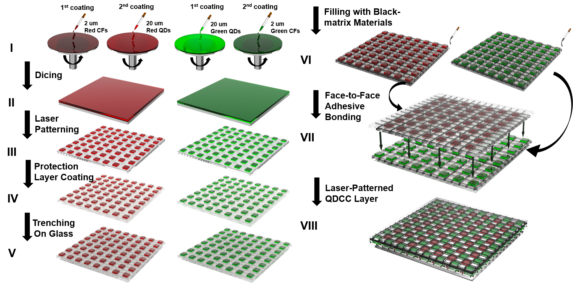
Fabrication of a Quantum Dot Color Conversion Layer (QDCC) by Laser Patterning for Full-color Mini/micro-LED Displays
Mini/micro-LED displays can be realized with the combination of red, green and blue (RGB) LED chips. However, mini/micro-LED displays based on RGB LED chips suffer from assembly yield issues which have hindered the technology from being embraced by major vendors. A quantum dot color conversion (QDCC) layer with monochromatic blue LED backlight arrays has proven to be a feasible alternative technology.
As the technology to fabricate the monochromatic blue LED backlight array with down-scaled pixels has become more mature, achieving a patterned QDCC layer with desirable converting lights has attracted increasing attention. However, saturated converting colors, adequate production efficiency and process stability are difficult to attain with traditional patterning methods of QDCC layers, such as photolithography or jet printing.
This project proposes a laser patterning approach to implement the QDCC layer for full- color mini/micro-LED displays. The proposed project provides a solution for the patterning approach and evaluates the optical performance of the laser-patterned QDCC. The innovative approach will result in a high production efficiency, a robust process, process scalability and saturated converting colors, which can provide a feasible solution for the implementation of full-color mini/micro-LED displays.
